🔍 Read the full analysis: What’s Beneath The Surface Of An AI Chip? on ThorstenMeyerAI.com

Get the little things that make your day delivered free with Prime
- Fast, free delivery on millions of items
- Prime Video, Amazon Music and more included
- Member-only deals all year
TL;DR
A November 22, 2026, explainer from ThorstenMeyerAI.com breaks down an AI accelerator as a layered package of compute dies, high-bandwidth memory, an interposer, substrate and liquid cooling. It argues that memory bandwidth and advanced packaging, alongside compute, shape performance and the supply of deployable AI systems.
ThorstenMeyerAI.com published an explainer on November 22 showing how current AI accelerators are assembled from compute dies, stacked memory, silicon wiring layers and cooling hardware—and how those packages fit into rack-scale systems. The report’s central point is that AI performance and availability depend not only on compute chips, but also on memory bandwidth, advanced packaging and manufacturing capacity.
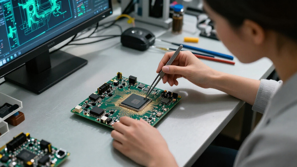
The explainer, by Thorsten Meyer, describes an accelerator not as a single chip but as a package of multiple components. Its layers include a package substrate, a silicon interposer that carries dense connections, compute dies, high-bandwidth memory (HBM) stacks and a cold plate for liquid cooling. Meyer says the accompanying 3D models show the layer order and component counts, but use schematic dimensions because the companies do not publish the relevant measurements.
Examples in the report show different approaches. It says Nvidia’s Rubin GPU uses two reticle-limited compute dies and lists 336 billion transistors, citing Nvidia’s architecture blog. AMD’s MI355X is described as combining eight vertically stacked accelerator complex dies with two I/O dies and eight 12-high memory stacks. These are manufacturer-specific designs, not a single standard layout for every AI accelerator.
The report explains that HBM places DRAM chips in stacks beside compute, connected vertically by through-silicon vias. A silicon interposer links those components with many connections in a compact area. On top, a cold plate carries liquid cooling: the report cites Nvidia documentation describing coolant flowing through plates attached to CPUs and GPUs in a tray.
Packaging Limits AI System Supply
The hardware layers matter because a fast compute die cannot do its work efficiently if data cannot reach it quickly enough. The explainer says memory bandwidth has risen from 900 GB/s for Nvidia’s V100 to 19.2 TB/s for Rubin, using figures attributed to Nvidia product information. Those figures refer to bandwidth per GPU across different products; they do not, by themselves, establish how much faster a model will run.
Packaging is another constraint. The interposer has to connect compute and memory at high density, and making larger, more complex packages at volume is a manufacturing challenge. The article cites TSMC’s CoWoS packaging technologies and notes that its larger CoWoS-L designs join silicon bridges in a carrier layer. That means availability depends on more than the number of compute dies manufacturers can produce.
For companies buying AI capacity, the combination can affect both how much computing equipment reaches the market and what it costs. The report cites SK hynix’s expectation that memory demand will exceed supply “through 2030.” That is a company forecast, not a guarantee of future shortages or prices. The article’s broader implication is that supply planning must account for memory and packaging as well as processors.
Products Worth Considering

Levoit Vital 100S-P Air Purifier with Washable Pre-Filter

Bose SoundLink Plus Portable Bluetooth Speaker, Black

Philips Hue Play Gradient Light Tube, Large, Black
As an affiliate, we earn on qualifying purchases.
From Chip Package to Rack
The report follows the accelerator from its base upward. A package substrate, a multilayer board in miniature, carries power and signals. Above it, the silicon interposer provides connections between the compute dies and HBM. The report quotes TSMC describing CoWoS-S as using a large silicon interposer to accommodate logic dies and HBM cubes. It says that CoWoS-S can accommodate an interposer up to about 2,700 square millimetres, or 3.3 times reticle size, according to TSMC.
For larger packages, the article points to CoWoS-L. It cites TSMC’s chief executive as saying on October 15, 2026, that the company was in “real world production of 5x reticle size” and working on 9x and 14x. The report also says AMD identifies CoWoS-L in its MI455X and MI450X designs. These statements describe company technologies and plans; they do not establish how many packages are being produced or delivered.
The system view makes the scale clearer. According to Nvidia’s DGX GB user guide, a GB200 or GB300 NVL72 rack has 72 GPUs and 36 CPUs, arranged in 18 compute trays, alongside nine NVLink switch trays, management switches and power shelves. The report says the rack also uses liquid cooling and cites Nvidia’s stated 120 kW cooling capacity for a GB200 NVL72. AMD’s platform is organized differently: the article describes eight OAM accelerator modules on a universal baseboard.
Published Dimensions Remain Unknown
The source report says Nvidia and AMD do not publish the physical dimensions of the dies, packages or memory stacks in millimetres. Its models therefore show schematic sizes rather than measured proportions. The article also does not provide independent production or shipment data to quantify how much interposer capacity or HBM supply is limiting accelerator deliveries.
Some figures describe different generations and products, so they should not be read as a controlled performance comparison. The reported bandwidth numbers indicate product specifications, not a benchmark of model response time. The SK hynix supply outlook is a forecast, while the scale of any resulting price effects for customers is not specified.
The source is a hardware explainer, not an independent audit of manufacturer claims. Its component counts, specifications and rack descriptions are attributed to company materials and technical documents. Actual configurations and availability may vary by product and deployment.
Watch Packaging and Memory Capacity
The next developments to watch are whether manufacturers expand HBM supply and advanced packaging capacity, and how those changes affect accelerator availability. TSMC’s stated work on interposers beyond five times reticle size and SK hynix’s demand forecast are relevant indicators, but the source provides no delivery schedule or production totals with which to measure near-term effects.
For buyers, the practical next step is to compare complete systems rather than compute specifications alone: memory capacity and bandwidth, package design, cooling requirements, rack configuration and actual supply all affect deployment. The explainer describes Nvidia’s Vera Rubin NVL72 as listed “Available Now” on Nvidia’s site, but does not provide shipment volumes or independently verify availability across markets. Those details remain open.
Key Questions
What is inside an AI accelerator?
As described in the report, it can include compute dies, HBM stacks, a silicon interposer, a package substrate and cooling hardware. The exact arrangement varies by product.
What does HBM do?
HBM is high-bandwidth memory made by stacking DRAM chips and connecting them vertically with through-silicon vias. It sits close to compute dies to move data between memory and processing components.
Why does packaging matter?
Advanced packaging connects compute and memory components using dense wiring in a compact package. The report identifies packaging capacity as a potential constraint alongside the supply of compute chips and memory.
How many GPUs are in an NVL72 rack?
The report says Nvidia’s GB200 and GB300 NVL72 systems contain 72 GPUs and 36 CPUs, along with compute trays, NVLink switch trays and cooling and power equipment.
Is the memory shortage expected to last through 2030?
SK hynix expects demand to exceed supply “through 2030,” according to the report. That is the company’s forecast; the source does not establish the precise scale of any shortage or its effect on prices.
Source: ThorstenMeyerAI.com